
What is the Photolithography Equipment Market Size in 2026?
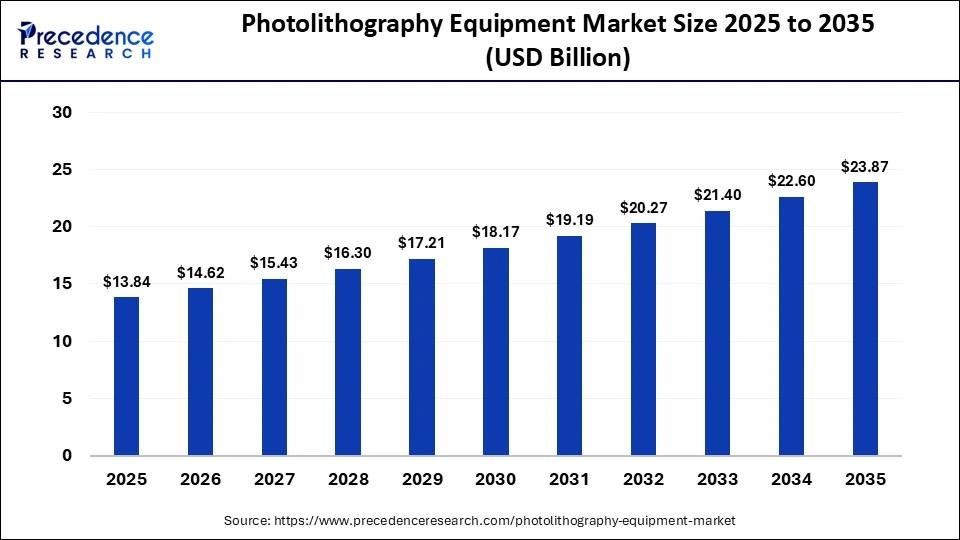
The global photolithography equipment market was valued at USD 13.84 billion in 2025 and is projected to grow from USD 14.62 billion in 2026 to approximately USD 23.87 billion by 2035, registering a CAGR of 5.60% during the forecast period from 2026 to 2035.
Market growth is being driven by the increasing demand for compact and high-performance electronic devices. This trend is accelerating the adoption of advanced technologies such as IoT, AI, and ML, which in turn is fueling the need for sophisticated semiconductor manufacturing processes. Additionally, continuous advancements in the semiconductor industry are further supporting the expansion of the photolithography equipment market.
Key Takeaways
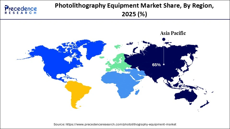
- Asia-Pacific led the global market with the largest market share of 65% in 2025.
- North America is expected to be the fastest-growing region in the foreseeable period.
- By process, the ultraviolet (UV) segment dominated the global market in 2025.
- By process, the deep ultraviolet (DUV) segment is expected to expand significantly in the foreseeable period.
- By light source, the excimer laser segment registered its dominance over the global market in 2025.
- By light source, the mercury lamp segment is expected to grow at a notable CAGR in the coming years.
- By wavelength, the 270nm to 170nm segment held the largest market share in 2025.
- By wavelength, the 370nm to 270nm segment is expected to show lucrative growth in the coming years.
- By end use, the integrated device manufacturers (IDMs) segment contributed the biggest market share of 59% in 2025.
- By end use, the foundry segment is expected to show the fastest growth over the forecast period.
What is the Photolithography Equipment Market?
The photolithography equipment industry involves the use of machinery such as extreme ultraviolet (EUV), deep ultraviolet (DUV), and i-line to transfer circuit patterns onto semiconductor wafers. The market also involves sales and servicing of tools to create microchips, along with paying attention to advanced packaging demand . The market is also abbreviated as the global trade of optical systems useful for semiconductor fabrication and other industries requiring precision work to transfer geometric patterns from a photomask onto a substrate. Such silicon wafers are treated with a light-sensitive chemical known as photoresist.
Market Scope
| Report Coverage | Details |
| Market Size in 2025 | USD 13.84 Billion |
| Market Size in 2026 | USD 14.62 Billion |
| Market Size by 2035 | USD 23.87 Billion |
| Market Growth Rate from 2026 to 2035 | CAGR of 5.60% |
| Dominating Region | North America |
| Fastest Growing Region | Asia Pacific |
| Base Year | 2025 |
| Forecast Period | 2026 to 2035 |
| Segments Covered | Process, Light Source, Wave Length, End-Use, and Region |
| Regions Covered | North America, Europe, Asia-Pacific, Latin America, and Middle East & Africa |
Regional Insights
Asia Pacific Photolithography Equipment Market Size and Growth 2026 to 2035
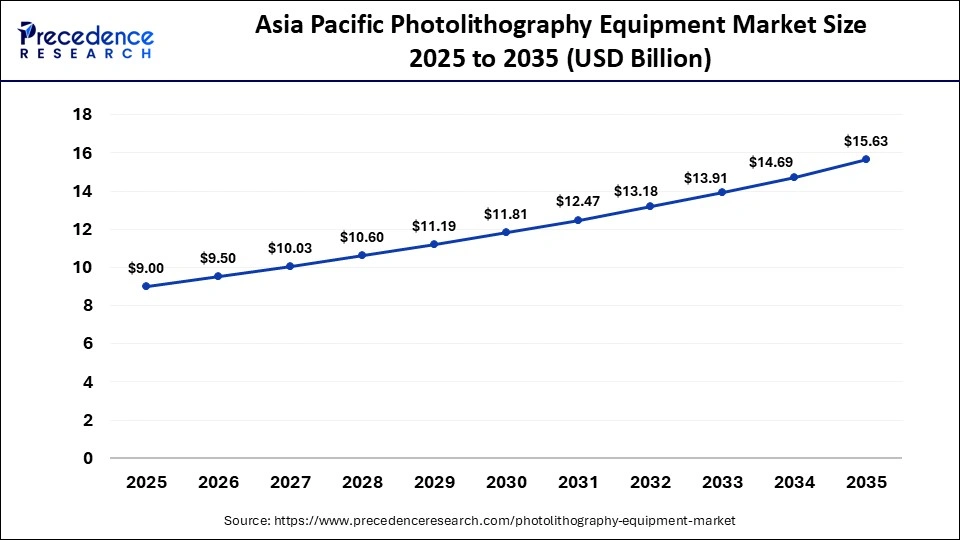
The Asia Pacific photolithography equipment market size is expected to be worth USD 15.63 billion by 2035, increasing from USD 9.00 billion by 2025, growing at a CAGR of 5.67% from 2026 to 2035.
Why Did Asia-Pacific Dominate the Photolithography Equipment Market?
Asia-Pacific held a major market share in 2025. Heavy investments in semiconductor manufacturing in various Asian countries are one of the major factors propelling the growth of the market. Growing demand for advanced lithography technologies, inclusive of EUV and DUV for advanced node fabrication, is also a major market driver. The demand for the market is also fuelled by factors such as 5G, AI, and IoT technologies, along with massive investments in advanced packaging.
Photolithography Equipment Market Companies
- ASML
- Shanghai Nikon Precision Machinery Co., Ltd.
- Canon Optical Equipment (Shanghai) Co., Ltd.
- Veeco Instruments Inc.,
- Conax Technologies
- TSMC
- Nikon Corporation
- SUSS Microtec SE
- Holmarc Opto-Mechatronics (P) Ltd
- KLA Corporation
Recent Developments
- In October 2025, Axelera AI unveiled its Europa chip, an AI processor unit (AIPU), designed to support high-performance edge computing use cases, including generative AI and computer vision applications. The chip features eight second-generation AI cores incorporating Axelera’s advanced Digital In-Memory Compute (D-IMC) technology.(Source: https://www.datacenterdynamics.com )
- In June 2025, Semiconductor Manufacturing International Corporation (SMIC), China’s leading chip producer, announced trials for the country’s first domestically produced advanced chipmaking equipment. The company is testing a DUV lithography machine to reduce reliance on U.S. imports and Western technology, and increase the production capacity of advanced AI processors. (Source: https://www.ft.com )
Segments Covered in the Report
By Process
- Ultraviolet UV
- Deep Ultraviolet (DUV)
- Extreme Ultraviolet (EUV)
- Others
By Light Source
- Mercury Lamp
- Fluorine Laser
- Excimer Laser
- Others
By Wave Length
- 370nm -270nm
- 270nm – 170nm
- 70nm – 1nm
By End-Use
- Integrated Device Manufacturer (IDMs)
- Foundry
By Region
- North America
- Latin America
- Europe
- Asia-pacific
- Middle and East Africa
Check this Report too: Ceramic Facades Market
Get this report to explore global market size, share, CAGR, and trends, featuring detailed segmental analysis and an insightful competitive landscape overview @ https://www.precedenceresearch.com/sample/8166
You can place an order or ask any questions, please feel free to contact us at [email protected] |+1 804 441 9344